This is a read-only archive of an earlier blog posting. Reasons for the
change are at http://blog.sensicomm.com.
The permanent version of this post - with comments (if any) - is at
http://sensicomm.blogspot.com/2014/02/hdmi-breakout-part-2.html
HDMI Breakout Part 2
I see the PCB in my Nov 6,
2013 post is getting some interest, so here's more info about it.
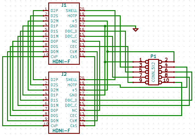
The image to the left is a Kicad screenshot. The breakout connector
(P1, CONN_5X2) is at the top, and pin 1 is the top right pad.
Odd-numbered pins on top, and even-numbered on the bottom.
Top connections are:
1 Ground
3
HOTP-J
5 DCC_D-J1
7 DCC_C-J1
9
CEC-J1
and the bottom connections are:
2 +5V
(J1 and J2 both)
4 HOTP-J2
6 DCC_D-J2
8 DCC_C-J2
10 CEC-J2
So to
use the board as a passthrough connection, add jumpers connecting
3-4, 5-6, 7-8, and 9-10. Obviously, it's NOT a good idea to have a
jumper connecting 1 and 2 (ground and +5V).
Here's the schematic. Pin 20 is the metal shell of the
connector, not a real pin.
Comments on blogspot.com
To make or view comments, see the original post at
http://sensicomm.blogspot.com/2014/02/hdmi-breakout-part-2.html